


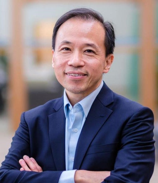
Voon Yew Thean
Faculty & Department
Joint Appointments
Professor, Office Of The Provost, Integrative Sciences and Engineering
Deputy President and Provost, Office of the Provost, Office of the Provost
Education
Doctor of Philosophy, University of Illinois, Urbana-Champaign, United States
Bachelor of Science with Hons, University of Illinois, Urbana-Champaign, United States
Bio
Aaron Thean is a Professor of Electrical and Computer Engineering at the National University of Singapore (NUS). He is currently the Deputy President (Academic Affairs) and Provost of NUS and was previously the Founding Dean of NUS College of Design and Engineering (2022), and the Dean of the Faculty of Engineering. In addition, he holds several technical leadership responsibilities at the University; which includes the Director of Singapore Hybrid-Integrated Next-Generation μ-Electronics Centre, Director of Hybrid Integrated Flexible Electronic Systems research program, and Co-Director for A*Star SIMTech-NUS Joint Lab on Hybrid Flexible Electronics. From 2016 to 2018, he had also served under the Deputy President of Research and Technology of NUS as the Director of Industry Engagement & Partnerships. In 2018, he was the Director of Applied Materials-NUS Corporate Laboratory for Advanced Materials. Prior to NUS, Aaron Thean was the Vice President of Logic Technologies at IMEC. Working with Semiconductor Industry leaders like Intel, TSMC, Samsung, Global foundries, Apple, and Sony, he directed the research and development of next generation semiconductor technologies and emerging nano-device architectures. Prior to joining IMEC in 2011, he was with Qualcomm’s CDMA technologies in San Diego, California. There, he led the Strategic Silicon Technologies Group. Aaron and his group worked on Qualcomm’s 20nm and 16nm mobile System-On-Chip technologies. From 2007 to 2009, Aaron was the Device Manager at IBM, where he led an eight-company process technology team to develop the 28-nm and 32-nm low power bulk CMOS technology at IBM East Fishkill, New York, from research to risk production. The technology was transferred successfully to several foundry partners, the technologies became the Industry’s first foundry compatible Gate-First High-k Metal-Gate with novel SiGe channel Low-Power bulk CMOS technologies. Aaron graduated from University of Illinois at Champaign-Urbana, USA, where he received his B.Sc. (Highest Honors), M.Sc., and Ph.D. degrees in Electrical Engineering (Edmund J. James Scholar). He has published over 400 technical papers and holds more than 50 US patents.
Contact Information


Semiconductor Chip Technology Microelectronics Artificial Intelligence Hardware Biosensors Heterogeneous Integration